
Newsroom


The demand for an ultrabroad optical material with a bandgap tunable from zero to at least 1~2 eV has been one of the driving forces for exploring new two-dimensional (2D) materials since the emergence of graphene, transition metal dichalcogenides and black phosphorus.
As an ultra-broadband 2D material with energy bandgap ranging from 0 to 1.2 eV, PtSe2 shows much better air stability than its analogue, black phosphorous. Although the angle-resolved photoemission spectroscopy (ARPES) technique and field-effect transistor electrical measurements have been used to investigate PtSe2, the exact transition point from semiconductor to semimetal is still in controversy.
Recently, a study led by Prof. WANG Jun from the Shanghai Institute of Optics and Fine Mechanics (SIOM) of the Chinese Academy of Sciences (CAS) investigated the superior nonlinear optical performance, ultrafast dynamics of layered PtSe2 and revealed its evolution signature from semiconductor to semimetal. This study was published in Laser & Photonics Reviews and selected as the inside front cover.
The researchers synthesized PtSe2 films with different thicknesses ranging from 4 layers to 55 layers by a thermally assisted conversion process. Then they studied the nonlinear optical performance and ultrafast dynamics using the pump probe technique with 380 fs laser pulses at 1040 nm with a repetition rate of 1000 Hz.
On the basis of nonlinear absorption results, they concluded that the bandgaps of all PtSe2 films were less than the excitation photon energy (1.20 eV), while the difference emerged in the ultrafast dynamics results.
The basic principle is that different nonlinear absorption signatures can significantly reflect the competition between the bandgap and the photon energy. For instance, the observation of two-photon absorption implies the bandgap is larger than the photon energy used, while saturable absorption implies the bandgap is smaller than the photon energy. Another crucial judgment basis lies in the lifetime of excited carriers, as it is on the different order of magnitudes for semiconductor and semimetal.
The scientists provide a viewpoint to characterize the semiconductor to semimetal transition from the perspectives of nonlinear optics and ultrafast dynamics based on a systematic investigation of samples with different thicknesses.
This study clearly demonstrates the evolution of nonlinear absorption and carrier dynamics with increasing layer thickness in PtSe2, indicating its promising potential in nanophotonic devices such as infrared detector, optical switches and saturable absorber.
This work was supported by the Chinese National Natural Science Foundation, the Strategic Priority Research Program of CAS, the Key Research Program of Frontier Science of CAS, the Program of Shanghai Academic Research Leader, Natural Science Foundation of Shanghai, Youth Innovation Promotion Association and President’s International Fellowship Initiative.
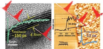
Fig.1 Ultrafast dynamics evolution from semiconductor to semimetal in PtSe2 (Image by SIOM)
Figure 2. Inside front cover (Image by Laser & Photonics Reviews)
