
In solid state materials, the electron has valley degree of freedom (DOF), based on which a variety of valleytronic devices such as valley filters and valves have been proposed. Valleytronic devices have the advantages of high integration density, high processing speed and low power consumption. For this reason, valleytronics has been one of the hottest research fields in recent years.
So far, optical valley excitation has been realized. However electrical means is still a critical challenge. In transition metal dichalcogenide (TMDC), the unique spin-valley locking relationship and the large valence band splitting strongly suppress the spin and valley scattering, leading to a long valley-spin lifetime in monolayer TMDCs. Therefore, it is expected that the valley DOF can be electrically controlled in TMDC/ferromagnet heterostructures.
Recently, a collaborated work by Prof. ZHANG Xiang’s group in University of California, Berkeley, and Prof. ZHAO Jianhua’s group at Institute of Semiconductors, Chinese Academy of Sciences, has demonstrated electrical generation and control of valley carriers in monolayer TMDC/(Ga,Mn)As heterojunctions for the first time.
As the spin splitting of TMDCs is manifested in the out-of-plane directions, p-type ferromagnetic semiconductor (Ga,Mn)As with perpendicular magnetic anisotropy has been employed as a spin aligner (Fig. 1). In order to obtain high-quality heterojunction, a site-specific dry transfer technique that allows precise placement of the exfoliated monolayer was developed. This method guarantees a clean interface between the monolayer and the MBE-grown (Ga,Mn)As film, which is crucial for spin injection.
Circularly polarized electroluminescence forming at the heterojunction between p-type (Ga,Mn)As and n-type monolayer WS2 at forward bias was captured as measuring signal, raised by the spin injected unbalanced carrier population at K and K’ valleys. The corresponding electroluminescence has been used as a reliable way to study optical transitions in monolayer TMDCs, as shown in Fig. 2.
This work not only realizes the electrical generation and control of valley carriers in monolayer TMDC, but also bridges the research fields of spintronics, valleytronics and 2D materials.
This work has been published online in Nature Nanotechnology on April 4, 2016.
The work in US was supported by MURI and NSF, and the work in China was supported by NSFC and MOST of China.
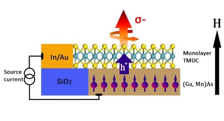
Figure 1. Schematic of the TMDC/(Ga,Mn)As heterojunction. (Image by Prof. ZHAO Jianhua et al.)
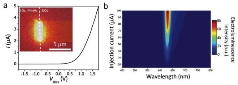
Figure 2. (a) I–V curve (inset: surface EL overlaid with the SEM image of the device), and (b) electroluminescence of WS2/(Ga,Mn)As device. (Image by Prof. ZHAO Jianhua et al.)

86-10-68597521 (day)
86-10-68597289 (night)

86-10-68511095 (day)
86-10-68512458 (night)

cas_en@cas.cn

52 Sanlihe Rd., Xicheng District,
Beijing, China (100864)
Copyright © 2002 - Chinese Academy of Sciences


