Newsroom


A research team led by Prof. LI Liang from the Hefei Institutes of Physical Science of the Chinese Academy of Sciences, in collaboration with Prof. ZHAI Tianyou from Huazhong University of Science and Technology, has developed an innovative "torsion unipolar barrier heterojunction" device that significantly advances polarization detection technology.
Their findings were recently published in Advanced Materials.
Polarization is a fundamental property of light, alongside intensity, wavelength, and phase. Compared to conventional intensity-based imaging methods, polarization enhances contrast and resolution. However, current on-chip polarization detection devices face two major challenges: limited spectral response in plasmonic and metasurface-based systems, and difficulties in simultaneously detecting the angle of linear polarization (AoLP) and the degree of linear polarization (DoLP) in low-dimensional anisotropic materials. Achieving wide-spectrum, high-precision polarization detection remains a pressing challenge in the field.
To address these limitations, the research team leveraged the unique anisotropic photoelectric properties of two-dimensional PdSe₂ to construct a dual absorption layer while precisely tuning the energy band of the intermediate MoS₂ barrier layer. This novel design enables bias-programmable control over carrier transport paths, leading to groundbreaking improvements in polarization detection.
The newly developed device features two key advancements. First, it exhibits bipolar photocurrent behavior at zero bias, allowing direct decoding of polarization-encoded bi-binary communication signals. Second, it eliminates the need for auxiliary polarizers, enabling real-time, simultaneous measurement of AoLP and DoLP, thus overcoming the limitations of traditional four-pixel array systems.
This study offers a fresh perspective on next-generation on-chip polarization detectors, simplifying device structures while enhancing optical information processing, according to the team.
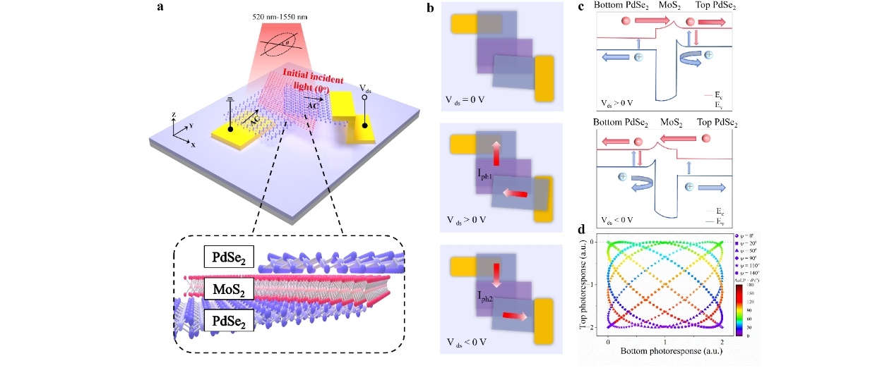
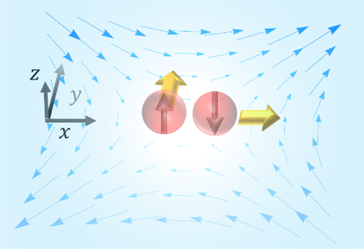
Schematic diagram of optical carrier transmission in PdSe2/MoS2/PdSe2 vdWH. (Image by MA Xiaofei)